Abstract
This paper presents the design and implementation of a low voltage, high efficiency class-E power amplifier (PA) for ISM band applications at 403 MHz. The PA circuit consists of an on-chip differential amplifier including the buffer stage on standard 0.35μm CMOS technology. The output matching circuit is implemented by off chip passive components including an external balun. The post-layout simulation results indicate that the amplifier is capable of delivering 20.9 dBm of output power to a 50Ω load with 1.5V power supply. The results also indicate that the PA has a gain of 11.8 dB at 403 MHz with power added efficiency (PAE) of 75%. The overall efficiencyincluding the buffer is 65.6%.
1. Introduction
The demand for single chip transceivers has motivated the design of power amplifiers in CMOS technology. Especially for short-range wireless applications that require moderate output power, CMOS amplifiers are the suitable choice. Various power amplifiers (PA) in CMOS technology have already been reported [1-4]. The mass fabrication cost of CMOS integrated circuits is relatively low; therefore, designing the whole system on a single chip is very cost effective. Considering the portable devices, an efficient power amplifier can provide long battery time. Therefore, increased efficiency is a prime requirement for future generation wireless systems. The major limitation with CMOS technology for high power applications is its low breakdown voltage and especially the situation is worse with deep submicron CMOS devices. However, with advancements in technology and the availability of high voltage CMOS transistors, this problem can be addressed. Thus, for wireless applications, with moderate power, CMOS is an appropriate choice. In this paper, a differential power amplifier is designed and implemented using standard 0.35 μm CMOS technology process. The paper outline is as follows. Section 2 briefly describes the operation and design principles of class-E power amplifier. Section 3 discusses the design and implementation details of the amplifier circuit. Simulation results are provided in Section 4 while the work is concluded in Section 5.
2. Class-E operation
Switching power amplifiers theoretically achieve efficiencies as high as 100%, but have drawback of poor linearity. Such amplifiers are suitable for systems with constant envelope modulation schemes [5-6]. The class-E PA is the most attractive candidate in terms of circuit simplicity and high-frequency performance. Typical configuration of a Class-E power amplifier is shown in Figure 1.

Transistor M1 operates as a switch and its current is passed through an inductor called radio frequency choke (RFC). The capacitance CS is in parallel with M1 and the parasitic capacitance of transistor is included inCS . LFIL and CFIL comprise a tuned circuit in series with a reactive component jX and the load impedance Ropt . The switch is turned on and off periodically at the input frequency. The LFIL -CFIL filter is tuned to the first harmonic of the input frequency and only passes a sinusoidal current to the load Ropt. The reactive component jX introduces the appropriate phase shift between the output voltage and the switch voltage to obtain desired waveforms [7]. The load network is designed such that the voltage across the switch is kept low when the switch turns off and voltage across the switch is zero when the switch turns on. The component values of single ended class-E power amplifier can be computed by following set of equations [8-10]:

Where VDD, Pout, ω, and Q are PA supply voltage, PA output power, PA resonant frequency and inductor Q factor respectively.
3. Design & Implementation
The major limitation of the CMOS technology is low breakdown voltage (VDS). In class-E amplifiers, the stress voltage at drain is 3.6 times VDD, therefore it is necessary to choose a device with higher VDS. For our design, we have chosen a high voltage NMOS transistor from standard 0.35μm CMOS design kit. This transistor has a maximum break down voltage of VDS=5.5V, and hence, with 1.5V VDD the maximum stress voltage on drain of the transistor is within safe limits, i.e., 5.4V.
3.1. Single ended class-E design
A single ended Class-E amplifier is shown in Figure 2. The circuit was optimized for an output power of 150 mW with an operating frequency of 403 MHz at a supply voltage of 1.5V. Simulation results indicate that the transistor width of 1800 μm is required in order to meet the output power requirements. The other component values were computed by (1-5) and finally optimized by CAD simulations.

3.2. Differential class-E design
Using differential topology gives some benefits over single ended configuration, such as common mode noise suppression. As a consequence, the even order harmonics are not significant. Differential design doubles the output power when compared with a single ended amplifier. For the same supply voltage and output power, the requirement on transistor size is also reduced in differential designs. This produces less parasitic capacitances and relaxes current consumption of the amplifier. Figure 3 shows the schematic of differential amplifier. The large inductors LRFC and LFIL are implemented off chip along with the external balun.

3.3. Buffer design
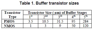
The width of amplifier transistor is as large as 1800 μm that produces high parasitic capacitances. Consequently, the input gate capacitance Cgs of the transistor becomes too large to be driven by the preceding stage of the amplifier. A buffer amplifier, in such cases is required to drive the amplifier. The buffer is designed by a chain of inverters connected in series to drive the large capacitive load of 6.864 pF. Each inverter is larger by a factor of K (tapering factor) than the preceding inverter. For known input and output capacitive loads, the optimum value of Kopt and total number of inverter stages required in the buffer chain can be determined. The input gate capacitance CL of the amplifier transistor is 6.864 pF. Total input capacitance of first inverter stage is 4 fF and the output capacitance of first inverter stage (unloaded) is 1.8 fF. Optimum number of inverter buffer stages N is calculated and results in N=6.7. A seven stage buffer is required to drive a load capacitance of 6.864 pF. However, the simulation results indicate that only a five stage buffer is sufficient as it does not degrade the performance. Sizes of each stage's PMOS and NOMS transistors are tabulated in Table 1.
3.4. Layout issues
On-chip realization of inductors LRFC and LFIL is not feasible as it occupies a large chip area. Therefore, external high Q inductors were used. The bond wire inductance is also taken into account. In differential architecture, the symmetry of on-chip components and dimensions of the interconnects play a very vital role in the performance to cater process variation. Since the design is a differential, it has two identical single ended circuits. The PA has potentially large currents in different parts of circuit, so wide and stacked interconnect structures are used. Transistors in the circuit have large sizes such as widths of 1800 μm. It is not viable to place such a large transistor in one dimension, as poly material has high resistivity than metal and becomes too resistive over long dimensions. Multi-fingers were used and folded for carving large transistors. The poly materials of the fingers are connected in parallel to significantly reduce the resistance. All drains of multi-fingers are interconnected to behave as one single drain. In a similar way, all sources are interconnected to provide one single source. To avoid cross-talk and interference at radio frequencies, different blocks are encapsulated with guard-rings. This helps isolating the blocks to minimize interference and decouple substrate noise. Adequate on-chip decoupling capacitors were also used. The layout for the differential amplifier is shown in Figure 4. The overall chip area is 0.56 mm2 (700x800 μm) including the pads.

4. Simulation results
The circuit simulations were performed in Cadence®. A test bench is designed to simulate the performance of PA. Pre and post-layout simulations were carried out.

Figure 5 shows waveforms at different nodes of the class-E PA after post layout simulations with RC extraction. Results indicate that the amplifier has a gain of 11.8 dB at 403MHz. Figure 6 shows power added efficiency (PAE) and output power as a function of input frequency. At 403 MHz, PAE of the PA is 75% and the output power is 125 mW. The overall efficiency including the buffer stage is 65.6%.

Table 2 shows the comparison of results with already reported similar power amplifiers.

5. Conclusion
The design and implementation of a low voltage high efficiency fully differential class-E amplifier is presented. Some key implementation issues have also been discussed. The post-layout simulation results are encouraging and indicate that the amplifier has potential to deliver 20.9 dBm of output power to a 50Ω load with 1.5V power supply. The results also indicate that the amplifier has a gain of 11.8 dB at 403 MHz with power added efficiency (PAE) of 75%. The overall efficiency including the buffer is 65.6%.
Hernández Caballero Indiana
Asignatura: CAF
Fuente:http://www.ewdtest.com/conf/proc08/ewdts08-68.pdf
No hay comentarios:
Publicar un comentario