Termination - the term brings to mind different values of resistance to different specialties in electronics. RF designers think about 50 ohm, video designers 75 ohm, audio and telecommunication designers 600 ohm - there are many possibilities. All of these termination resistor values have a common purpose - they match impedances in the circuit and therefore attenuate reflections that would otherwise cause problems in the system.
This article will focus on 50-ohm terminations - but this has more to do with the test equipment available in the author's lab than a preference for RF applications. The techniques established here are applicable to any value of termination resistor, because the electrical laws governing them are universally applicable to other resistance values.
For every input termination resistor, there needs to be a companion series-matching resistor in the source. A laboratory signal source will be assumed. Laboratory sources can be thought of as an ideal voltage source (zero ohm output impedance) in series with a 50 ohm resistor. This resistor is shown as Rs in the schematics below. Laboratory sources assume a 50 ohm termination in the circuit that is driven, and take it into account when generating their display.
For example, a laboratory source is set to 1 Vpp. An ideal source (internal to the instrument and inaccessible to the user) produces a 2 Vpp output. This 2 Vpp output is applied to the internal 50 ohm series-matching resistor. If the source is monitored with a high impedance-measuring instrument -V an oscilloscope with a 1 M-ohm input, for example, it would produce very nearly 2 Vpp - even though the output indicator on the instrument indicates 1 Vpp. When the same source is monitored with an instrument that has a 50 ohm input, the output would be 1 Vpp because Rs and Rt produce a 2:1 voltage divider at the circuit input.
It is very important to realize that the only voltage available to the instrument user is the voltage at its output connector (after the 50 ohm source resistor). Instrument accuracy is only as good as its internal accuracy, as modified by the input termination resistor of the circuit.
It is worth a brief mention that 50 ohm is not a standard one percent resistor value. The closest standard value is 49.9 ohm, and this value has been used in the examples below.
Four cases will be covered in this article: Inverting Stage attenuators Non inverting stage attenuators Single-ended to fully differential stages Differential to fully differential stages
Single-Ended Op Amps
Single-ended op amps are a mature technology - therefore some of what is presented here may be a review. The inverting case, however, is subtle and needs explanation. Inverting Stage Attenuators
Consider the circuit of represented in Figure 1. It assumes a laboratory source as described above. Most designers assume that the 49.9 ohm termination resistor, combined with resistors Rg and Rf will guarantee a gain of 1 - but wait! The real story is a little more complicated.

Figure 1. Inverting Gain Stage
Assume that the signal source is a laboratory source set to 1 VPP. Both Rg and Rt affect the level of voltage applied to the circuit. The function generator indicates a level of plus-minus 0.5 V (1 VPP) - while only plus-minus 0.484 V (0.968 VPP) is applied to the board. The user might wonder, "what happened - where did the rest of the voltage (plus-minus 0.016 V) go"?
There are two ways of looking at this problem:
From the function generator side. The function generator contains a 50 source resistor. The EVM contains a 49.9 ohm termination resistor, and therefore the output of the function generator will see (approximately) a 2:1 voltage divider. The function generator anticipates this, and scales its output accordingly.
In the inverting configuration, however, the inverting input presents a ground potential to the gain resistor Rg. This is because the ideal op amp model forces both inputs to the same voltage potential. The non-inverting input is connected to ground, and therefore the inverting input will also be at ground. The resulting impedance resistance for the stage will therefore be equal to the termination resistor in parallel to Rg, in this case 750 ohm. Therefore, the instrument output is actually:

This can also be viewed as the Thevenin equivalent voltage looking into the source at Rt.
From the circuit side. The Thevenin equivalent resistance of the circuit plus the source - looking towards the source from the inverting input of the op amp is:

Therefore, the inverting gain on a 0.5 Vpeak ideal voltage source (assumed to be embedded in the function generator) is:

The two results are equivalent.
Non-Inverting Stage Operation
The circuit of Figure 2 contains a 50 ohm terminated input (Rt), and gain setting resistors. Because Rt does not appear in parallel with Rg as in the inverting case, the gain calculation is much simpler - and the termination resistor does not affect the gain expression that the designer is probably familiar with:


Figure 2. Non-Inverting Gain Stage Figure
Fully Differential Op Amps
Fully differential op amps present some special challenges for terminated operation, because they should have two balanced feedback loops for symmetrical operation. Termination presents some special problems for this requirement.
Two cases will be discussed. One is single ended signal input, the other fully differential signal input.
Single-Ended to Fully Differential Conversion
Termination is applied to one of the two inputs - the other input is grounded as shown in Figure 3. This automatically creates an imbalance in the two feedback loops. Some of the reasons are described in the section above - all of that analysis applies to the bottom feedback path.

Figure 3. Single-Ended to Fully Differential
The overall effect, of course, is to place 25 more ohms on the bottom feedback path than on the top (Rs || Rt + R3). This means that the gain on the bottom feedback path is less than that of the top. So, 25 ohms must also be added to R1. But this changes the gain of the entire circuit to less than 1, so both R1 and R3 must both be decreased to boost the gain. This could go one and on - the design is an interactive process. To simplify this task for designers, Texas Instruments provides an on-line calculator on its web site. This tool can be accessed either through the Analog and Mixed-Signal Knowledgebase, or through the Engineering Design Utilities section on the Analog and Mixed Signal portion of the TI web site.
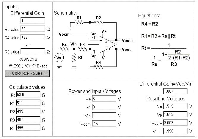
Figure 4 shows a screen shot of the fully differential amplifier component calculator.
The fully differential component calculator has six panes. Data entry is primarily made in the upper left pane, although the bottom middle pane contains some secondary entry fields.
The top middle pane contains the schematic for a terminated single-ended to fully differential conversion. Design equations are shown in the upper right hand pane. The equations for RR3,R4 and Rt are interrelated through the ''A'' parameter. The tool will make a preliminary calculation to get close to the correct values, and then it will refine the calculation and ''goal seek'' to the final value. The execution time depends on the step size used in the goal seeking calculation, and therefore selecting ''E96'' resistor values will execute much faster than ''Exact'' values. The designer should be patient, because execution times of several seconds or longer are possible, especially if gain is changed radically when ''Exact Values'' is selected. The designer selects the desired gain and the impedance of the signal source (default value of 50 ohms). The designer then has the option of selecting a seed value for either R3 or R4 (but not both). If the designer attempts to select both, only the last value entered will be used for calculation.
Almost without exception, the designer should initially try to select the value of R4, because it is often specified on the data sheet. The designer should experiment with R3 only if the recommended value of R4 does not yield an acceptable design (the tool has internal limits set to resistor values that make sense for real designs).
When the designer selects ''Calculate Values,'' the tool will calculate resistor values in the bottom left pane and circuit simulation results in the bottom right pane. If the designer wishes, the power and input voltages can be changed in the bottom middle pane, and these will affect the simulation results in the bottom right.
Note that this tool provides dc operating point only - it does not give ac simulation. Nevertheless, it will save the designer a lot of grief trying to do it the ''brute force'' method.
The implementation of Figure 5 is completely equivalent to that of Figure 3, it does not matter which input is used for the signal.

Figure 5. Alternative Single-Ended to Fully Differential Conversion
Fully-Differential In/Fully-Differential Out
Consider the circuit of Figure 6. In this configuration, input termination (resistor R1), is used to terminate a fully differential input.
Fully differential gain for the un-terminated case is determined by the relationship:

Where Rf is R3 in the top feedback loop and R6 in the bottom, and Rg is R2 on top and R5 on the bottom.
The designer should recognize the gain expression as being very close to the expression for the single-ended inverting stage (but without the negative sign). There is no negative sign because it is meaningless when both polarities of output are simultaneously available.

Figure 6. Fully Differential Operation
When a termination resistor is used, it affects the gain in a manner similar to the single-ended cases. In this case, however, the effect is not as intuitive.
Figure 7 shows the input of a differential stage as an ideal voltage source, with its characteristic 50 ohm source impedance split in two parts, between a "phantom ground". The termination resistor is also shown in two parts between the same phantom ground. The end result is the two 25 ohm resistors above the phantom ground appearing as a single 12.5 ohm resistor (the parallel combination). This 12.5 ohm resistance appears in series with the top Rg, changing the gain. Similarly, the two 25 ohm resistors below the phantom ground add to the bottom Rg, changing the gain and balancing the top gain.

Figure 7. Fully Differential Operation
The gain of the fully differential stage, therefore, is:

For the circuit of Figure 6, the differential gain is:

Changing the gain is much more straightforward than in the previous case, because equal changes made to the top and bottom feedback loop simultaneously are inherently symmetrical.
Output Series Resistor Matching
The circuits shown above can also be considered to be voltage sources. The output impedance of most op amp circuits (operated in a closed loop) is low enough that it can be considered to be zero. Therefore, it is a good approximation to consider closed loop op amp to be an ideal voltage source.
The reader is reminded that in the discussion above, an ideal voltage source is assumed to be at the heart of a laboratory voltage source. Therefore, by extrapolation, the reader hopefully sees how to cascade terminated stages - by adding 50 ohms in series with the op amp output to create a 50 ohm "source" for the subsequent stage.
This is often the case in RF design, where each stage has 50 ohm input and output. If the circuits above drive a 50 ohm load, they need a 50 ohm resistor in series with the op amp output. This will, of course, create a 2:1 voltage divider (-6 dB) with the termination resistor in the subsequent stage. This has to be taken into account in the design of overall system gain. It takes 6 dB of stage gain to compensate for a 2:1 voltage divider. The -20 dB per decade slope of the open loop response of a typical voltage feedback op amp, combined with 6 dB of gain forces a designer to choose a part with approximately four times the bandwidth that would be required for a unity gain stage.
The proper application of termination is a powerful way of suppressing reflections in high-speed circuits. It comes with a price; however, it introduces voltage dividers that attenuate the signal. Stage gain has to be increased to compensate - and that often times dictates a much higher bandwidth part to accommodate the additional gain required.
Termination can introduce subtle gain errors into a circuit if it effects are not properly taken into account. The rules governing termination are simple - Ohm's law, the voltage divider law, and the superposition principle - therefore it is not asking a great deal from analog designers to do the calculations. The only exception is the case of termination a single-ended to fully differential conversion, and Texas Instruments has provided a utility to simplify the task.
Hernández Caballero Indiana
Asignatura: CAF
Fuente:http://www.planetanalog.com/story/OEG20020724S0082
Asignatura: CAF
Fuente:http://www.planetanalog.com/story/OEG20020724S0082
No hay comentarios:
Publicar un comentario